Thursday, 29 January 2015

Arduino MRF24J40 Wireless Shield

We will equip Arduino with wireless connectivity basing on MRF24J4 module by Microchip. As a sample application, we will remotely control a relay, operated by a floating input, and we will virtualize the Arduino USB serial port.
The MRF24J40MA radio module is manufactured by Microchip, that also provides useful and complete software libraries (identified as MiApp) for module management (creation of a complex wireless network, network identification, device addressing, sending and receiving data, etc. …). Clearly, Microchip provides those libraries free of charge only if they are compiled with MPLAB (Microchip C compiler and development environment) and executed in a Microchip CPU (PIC microcontrollers).
On other hands, Microchip provides the data-sheet of all its devices (MRF24J40MA included) and the complete knowledge base for their management. So, nothing prevents you from deeply study the data-sheet and, starting from zero, write down your own libraries for the CPU and development environment you want to use.
From these considerations, we decided to start the project that we are presenting on these pages whose ultimate goal is to use the wireless module MRF24J40MA with an Arduino hardware platform. The additional shield we developed, to have the radio module and all its components working properly, has also an output relay and an opto-coupled input. The rationale behind this choice is to equip the shield not only with the radio part but also with at least a pair of input / output so that it could be more than enough for simple applications.
Regarding our newly developed software libraries for Arduino, those cannot fully cover all of the features offered by the Microchip proprietary libraries (that allow you to create different types of networks, broadcast communications, etc ….). The operations already available are enough for the basic management of a WiFi network: module initialization, setting of network PAN ID, set the node network address, transmit and receive data. Because of these differences between Arduino and Microchip libraries, some features have been simplified. In particular, we have removed the distinction between Coordinator and End Device node but hierarchically all nodes have the same level and offer the same functionality. Maybe you lose some application optimization but surely, you have huge advantages (which, in our opinion, largely cover the disadvantages) from the point of view of simplicity and ease of use.

WiFi Hardware Chip 
MRF24J40 is a RF transceiver, compatible with 2.4GHz IEEE 802.15.4 standard.
For our applications, we will use the full version of the module (MRF24J40MA) that besides the transceiver integrates also a tuned antenna, quartz and other external components required for WiFi communication. It has a mechanical strip shape, 2,54mm step and has already passed all wireless required certifications.
To interface with an external MCU it has an SPI port, interrupt, wake and reset pins; there are also pins for power feed.
The access to the various radio functions is through the read / write of a long series of internal chip registers (for details, please consult the full product description). Our libraries shall manage these registers, hiding at Arduino application level the implementation details but offering the general function calls for configuration and communication.

Arduino MRF24J40 Library

The MRF24J40 libraries for Arduino offer some basic functions of wireless network configuration and communication. They have not all the features of Microchip MiApp but there are all the necessary functions to set up a WiFi network, to address nodes and to allow direct data exchange between them.
The library provides an object called Mrf24j for the complete WiFi stack management. The object constructor gets as input the number of Arduino pin to be used for reset, chip select and radio module interrupt (the SPI port is the default, ie pins 11, 12 and 13 for the Arduino Uno).
There is a reset function that, through the reset pin as defined above, resets the chip (best practice is to reset hardware every time the software starts) and a Init (to be called after the reset) that initializes the SPI port and the registers of the radio module.
To work properly and to exchange messages, every node needs to specify which WiFi network (PAN ID, clearly the same for all) they belong and which is its unique network address. To set the PAN ID we have to use two functions (void set_pan (word PANID) and word get_pan (void)) that respectively write and read the PAN ID chosen.

Instead to configure nodes addresses, we will use void address16_write (word address16) and word address16_read (void) (since the variable is a 16-bit word, we cannot have more than 256 nodes in the network).
Other config functions that may be useful are:

void set_channel (byte channel) that allows you to specify what radio channel to be used;
void set_promiscuous (boolean enabled) that allows you to configure whether to use normal or promiscuous rx (i.e. if you want to receive any packets from the channel);
void rx_enable(void) and void rx_disable (void) that respectively enable or disable the receiving section;
void set_palna (boolean enabled) that allows you to enable the external controller PA / LNA;
void set_bufferPHY (boolean bp), which allows to enable the receival of both user data and physical communication payload.
Let us check how the communication works and the functions involved. The first thing to say is that the whole mechanism is implemented in a special way using Arduino CPU interrupt. This implementation is perhaps a bit more difficult than usual but allows you to manage everything more efficiently involving the Arduino CPU only when necessary.
The radio chip has a pin that sends an interrupt to the CPU to indicate that it has data ready; The Arduino software must be written to handle the interrupt indicating what to do in these cases. As we shall see later by analyzing the source code, we use the Arduino attachInterrupt to indicate which function must be executed when a “change interrupt” occurs from the MRF radio interrupt pin.
The software library contains the function void interrupt_handler(void) called directly by the specified interrupt handler. The handler reads all the data from the radio module and makes it “available” again to receive further information.
Other things to define are the two functions that respectively receive and transmit data. Once you have defined these functions, the MRF24J40 library offers the methods void check_flags (void (* rx_handler) (void), void (* tx_handler) (void)) that must be called cyclically (typically in the method loop ()) to manage properly the defined handlers, avoiding overlapping between Rx and Tx.

Finally, the real functions for transmitting and receiving are respectively void send16 (word dest16, char * data) that needs parameters like network address of the destination node and the pointer to the data buffer to be transmitted and rx_info_t * get_rxinfo (void), which returns a pointer to a structure type rx_info_t specially defined to encapsulate all the information received.

Electrical Wiring


The hardware is based mainly on the WiFi module MRF24J40MA (chip U1). The radio chip needs to be managed by a main CPU through the SPI port, to receive commands and send responses. The SPI port is located on pins 5, 6, 7 and must be connected to Arduino SPI pins (SCK, MISO and MOSI).
The radio module requires a power supply of 3.3V, while the Arduino digital port works at +5V, so you cannot make a direct connection but you must match the right voltage levels. Our choice fell on an integrated circuit designed for this purpose, the chip 74HC4050D (U2 chip in the diagram). Since all the connections between Arduino and MRF24J40MA need different voltages, we will convert all of them through the 74HC4050D.
In addition to the SPI port, the radio chip also provides the Wake, Interrupt, Reset and Chip Select pins. The Wake pin is directly connected to the positive voltage level because we choose to keep always the radio on.
The Interrupt pin is connected to Arduino D2 digital port; this is because Arduino can control the pin D2 via an interrupt and, as we can see by analyzing the sketch source code, this mechanism allows a more efficient resources management.
The other two pins (Reset and Chip Select) can be operated from any other Arduino digital port; to leave a certain amount of freedom of choice (in order to be ready for further development or additional shields), we have prepared two solder bridges to each pin; by soldering one of them, you can make your own choice.
Finishing the radio module analysis, we note the 100nF capacitor C3 connected to the WiFi chip power pin (as required by the data-sheet) and the presence of a LED (green LED in the diagram) connected to the Chip Select pin of MRF24J40MA itself (in order to get the visual indication of the presence of the communication).
With regard to the communication part of the electric scheme, the analysis is done; however, we choose not to implement a simple transmission shield but equip it with at least a minimum set of input and output. In particular, we have provided a photo-coupled input (based on the photo-coupler 4N25) and an output relay (RL1 relay driven by BJT T1 stage). Also for these I / O, we decided to leave freedom of choice about which Arduino port to be used (always using the technique of the two solder bridges).
Testing
To test this sample application you need to have at least two systems MRF24J40 + Arduino Shield.
To program Arduino we use the same procedure through IDE; but first you need to modify the source code to fit the hardware pin-out chosen and change the network addresses of the two nodes. In particular, replace the variables pinResetMRF, pinCSMRF, pinShieldRele and pinShieldInput; thisNodeAddress and destNodeAddress to define source / destination nodes.
At this point you are ready to turn the system on and play with it. Try to change the status of an opto-coupler and verify that the relay of the other shots. Finally, connect with different USB cables a PC to one card; open on the PC a serial terminal (HyperTerminal or similar,”connected” to a different virtual COM port), select the configuration 9600, 8, N, 1 and no flow control and check that when “writing” the data in a window (remember that if you do not have local echo enabled you do not see what you type), these are transmitted and received on the serial port by all cards.

MP3 Player with FM Radio

This circuit is used for playing MP3 files from a memory chip, card reader or from a pen drive. Same circuit is also used for receiving telecast of FM band Radio with digital Display of frequency.
You will need MP3 Kit.
Kit include MP3 Card with Digital Display, USB port, Remote Control and connecting cables as shown in the fig below

Receiver
For Simplicity of the Circuit we have omitted panel button which is marked K1,K2,K3 and K4 on PCB. All function is included in remote.
Circuit Diagram of this project will be available soon.
You have to Connect an Arial for proper functioning of FM Radio. Soldering point of Arial is given on MP3 board.

Tuesday, 27 January 2015

Interface a SD Card Using

The microcontroller systems may have to back up the data which they have read during their operation or the data which they need to access during their running time. Most of the microcontrollers have built-in EEPROM memory but they come in comparatively small sizes. In order to use the microcontroller in applications like file accessing, media player etc. an external memory card is necessary. The SD memory card comes in large storage capacities ranging from 1 GB to 8 GB and they are compatible with the SPI bus of the microcontroller. The large storage capacity and simplicity in interfacing results in wide usage of SD memory card by the microcontrollers. The files in an SD memory card are stored using FAT32 or FAT16 and one should use the code or FAT file-system library to access the files from an SD card.
The easy prototyping platform Arduino provides a library for accessing the SD memory cards. This particular project explains how to interface a SD card using an Arduino board and perform some read and write operations on it.

Saturday, 24 January 2015

DC Electronic Fuse

This DC electronic fuse never needs to be replaced. It can be repaired with just a single press of the start/reset button S1. Once S1 is pressed, the thyristor T1 triggers and the current flows to the consumer load through T1 and resistor RS. Even after releasing the start button, the current continue to flow as long as the current’s value does not sink below a certain level
The current flowing through the thyristor T1 will sink below the holding level when the current is rerouted through the transistor T2 2N3055. T2 and RS are built into the electronic fuse circuit for this purpose. If the voltage drop at RS exceeds above base-emitter-diode trigger voltage of the T2, the transistor conducts thereby bypassing the thyristor. The resistance value of RS must be at least 0.2 W. It must be dimensioned that the product of RS multiplied by the fuse current value equals to 0.7 volts.
Once T2 bypasses the T1, the current flowing through the thyristor sinks below the holding level and the T1 shuts off. This in turn causes the voltage drop at resistor RS to sink below the base-emitter trigger voltage of T2 and the transistor shuts off. The end result is the shutting off of the whole circuit. The DC fuse can be reactivated by pressing the start/reset button.
The value of resistor R1 is dependent on the supply voltage. Multiply the supply voltage with 1 KW to get the value of R1. Connect the dc electronic fuse circuit to the PLUS line of the consumer load. THe coltage drop at the circuit is less than 1 volt.
DC fuse PCB layout

Wednesday, 21 January 2015

Arduino & Raspberry Pi Camera Interface

Yes,we learned that we can take mobile phone camera modules from almost all mobile phones to inteface them with our advanced hobby electronics projects just as with any other standard add-on modules. Since this calls for an appropriate microcontroller, it is better to use Arduino or Raspberry Pi microcontroller as a utile platform.
Raspberry Pi camera
Recently I’ve received a Raspberry Pi camera board. The camera, comes with a ribbon cable already attached to it,is a small size (25mm x 20mm x 9mm) board where a fixed focus 5MP camera module is attached. Part number of the camera module (from OmniVision) is OV5647. At the heart of the OV5647 camera module is a 1/4” color CMOS QSXGA (5 megapixel) image sensor with OmniBSI ™ technology. This Raspberry Pi camera module can be used to take high definition video, as well as stills photographs. It is easy to use for novices, but has plenty to offer advanced users looking to expand the knowledge.
Raspberry PI comes with two first-rate connectors on board. One is between Ethernet and HDMI, and the other is near GPIO. The one closer to Ethernet connector is Camera Serial Interface (CSI ). This CSI is directly connected to the Raspberry Pi GPU which can process images without ARM intervention 
While connecting the camera module to the CSI port (located behind the Ethernet port) of the Raspberry Pi board,ensure that camera cable is inserted in right way, ie the blue strip in the flexible cable is towards the Ethernet (LAN) port. Once you are connected,enable the camera software, test the camera and try using it with Bash or Python. As I am a newbie in the Raspberry Pi world, I haven’t drudged enough into all features and capabilities of my borrowed Raspberry Pi (and the camera module). If you want to leap into the future of amazing possibilities, have a look at the documentation
The Raspberry Pi camera board transfers data through an extremely fast camera serial interface (CSI-2) bus directly to the system-on-chip (SoC) processor. It does this through a 15-pin ribbon cable, also known as flexible flat cable (FFC), and connects to the surface mount ZIF 15 socket in the Raspberry Pi board. As you may noted, the camera module on this official Raspberry Pi camera board is identical to the camera modules (ccd imagers) found in many mobile phones
Luckily, most of the mobile phone cameras are not only MIPI compliant but also CSI compliant (see the first part of this article). The 15-pin Raspberry Pi CSI interface connector pinout is also included here to help you to keep proceed with your tinkering ideas. Note that, in Raspberry Pi, there are two flexible Flat Cable (FFC) connectors (S2 & S5). S2, near to the micro USB connector, is the Display Serial Interface (DSI). It allows low-level interfacing with LCDs and other displays with Raspberry Pi. It is a 15-pin surface mounted flexible flat connector, providing two data lanes, one clock lane, 3.3V and GND. S5, located between LAN and HDMI connector is the MIPI Camera Serial Interface 2 (CSI-2) connector for camera modules. It is a 15-pin surface mounted flat flexible connector, providing two data lines, one clock lane, bidirectional control interface compatible with I2C, 3.3V and GND. The data transmission interface in CSI is unidirectional differential serial interface with data and clock signals (the physical layer of this interface is the MIPI Alliance Standard for DPHY).
Arduino camera
Adding a camera to your Arduino UNO is not very difficult, because ArduCAM ™ Shield is infront of you. You can find a good tutorial on ArduCAM here
This tutorial will demonstrate how to use the ArduCAM shield on Arduino UNO board, aim the point and press a snapshot button you will get a BMP picture saved on the SD/TF card!
ArduCAM shield hardware integrates all the necessary components to interface with camera modules. User only need a extra support camera modules and a TF/SD card to start image capture. The ArduCAM shield includes a ArduChip which handle complex timing between MCU and LCD, Camera, FIFO. It exports a standard SPI serial interface and can be interfaced with wide range of microcontrollers. Further, ArduCAM shield includes two sets of pin out, identical in function. One is Arduino standard, it can be well mate with standard Arduino boards like UNO, MEGA2560, Leonardo and DUE etc. The other one is alternative port which can be connect to any platform like Raspberry Pi. After the great success of ArduCAM shield Rev.B, the ArduCAM team now released a more powerful ArduCAM shield Rev.C with amazing new features. This revision supports camera modules including OV7660, OV7670, OV7675, OV7725, OV2640, OV3640, OV5642 and MT9D111.
CMOS image sensor interface divided into two classes, one is DVP (Digital Video Port) interface, the other is MIPI Mobile Industry Processor Interface. The main difference between DVP and MIPI is that DVP is parallel interface and the MIPI interface is high speed differential serial interface. MIPI interface provide higher data band width than DVP interface and support higher resolution and frame rate
Image sensor is usually cheap and you can buy them for as little as $5.00 on eBay. However, when it turn into a “microcontroller-compatible camera module”, the finished board costs a lot more. In conclusion, I would have to say that it is worth spending time and effort to make your own camera modules, because the experience of reverse engineering and hacking is really interesting (at least for me). This is just a starting point, as promised I will come back with useful updates in near-future


XL6009 12V Universal Charger for Laptop/Notebook

I recently failed to resist buying a compact power module from eBay for almost nothing! As usual, thereafter I leaped into the inside electronics of the module, and really amazed by the hidden magic power of that little board. Yes, a simple but highly useful dc-dc boost converter block, literally, suitable for unlimited practical applications!
At the heart of this improved dc-dc boost converter is IC XL6009, which is a 400KHz 60V 4A Switching Current Boost/Buck-Boost/Inverting DC/DC Converter chip, specially design for portable electronic equipment applications. XL6009 can be configured as either a boost, flyback, SEPIC or inverting converter. The XL6009′s built in N-channel power MOSFT, fixed frequency oscillator, and the current-mode architecture results in stable operation over a wide range of input and output supply voltages. This chip, from XLSEMI, is available in TO263-5L package.


Fortunately, well-documented datasheets of XL6009 are available in the web, enough for a good insight. After the walk-through, I revert to my eBay module and drawn the schematic diagram of the module just for an evaluation. Here it is


According to XL6009 IC datasheet, this module’s output voltage can be calculated using the formula Vout = 1.25x(1+R/1K), where R is the value of the potmeter. Any idea spark? Yes, now it is very easy to output a high-current DC supply voltage near 19VDC, from an input supply voltage of 12 VDC!
The findings shed some light on the fact that, with the help of this module, it’s very easy to build a Universal Laptop/Notebook Charger for in-car applications. As an aftereffect, I build a compact Universal Laptop/Notebook Charger wired around the XL6009 module as shown in the next circuit diagram.
This charger receives 12VDC supply input from the car battery through the in-dash cigar lighter socket, and gives powerful DC voltage output for energizing the connected laptop/notebook computer. Built-in 0-30V digital voltmeter module (DVM) – another fancy item from eBay – simplifies the output voltage setting task.
Remember to set the output voltage to a default value of 19VDC using the 100K (incircuit value of 50K) potmeter. Finally, attach your own standard/custom laptop/notebook power cable with proper connector (dc power jack) at the output of the universal charger.
Test Result:
  • Input Voltage: DC12V/5A (from lab power supply)
  • Output Voltage: DC 19V (pre-setted)
  • Output Current: 1.5 A (typical)
  • Input Voltage: DC12V/5A (from lab power supply)
  • Output Voltage: DC 15V (pre-setted)
  • Output Current: 2.0 A (typical)


Arduino 8×8 LED Matrix

8×8 LED Matrix modules are now widely available, and fortunately they are easy to use with our favorite Arduino microcontroller. 8×8 LED Matrix module have many applications in real life, such as various types of electronic display panels.
The LED matrix can be driven in two ways (parallel or serial). Here we drive it in the serial manner in order to save interface (needs only three data lines). The serial-driven LED matrix actually dynamically displays the LEDs (row-by-row or column-by-column). The persistence of vision for humans is about 0.1s, so as long as we can serially display all 8 rows/columns within 0.1s, we’ll see a complete character or pattern.
Our project is infact an Arduino with Serially Interfaced MAX7219 Operates an 8X8 LED Matrix to display a heart pattern. The MAX7219 IC is a serial input/output common-cathode display driver that interfaces microprocessors to a 7-segment numeric LED displays of up to 8 digits, bar-graph displays, or 64 individual LEDs. For convenience, here an 8×8 LED matrix, integrated with a MAX7219 IC setup, available as a pre-wired module is used. Typical specification of this LED Matrix Module is shown below:
  • Operating Voltage: DC 4.7V – 5.3V
  • Typical Voltage: 5V
  • Operating Current: 320mA
  • Max Operating Current: 2A 

 
Wiring Instructions
  1. Connect Arduino pin8 to DIN on 8×8 LED Matrix
  2. Connect Arduino pin9 to CS of 8×8 LED Matrix
  3. Connect Arduino pin10 to CLK of 8×8 LED Matrix
  4. Connect an external 5VDC (1A) to VCC of 8×8 LED Matrix
  5. Connect external 5VDC supply’s GND, to the GND of 8×8 LED Matrix Module
Note that the 8x8LED Matrix Module should be common-grounded with Arduino, ie, always remember to interconnect the Arduino GND terminal with the external 5VDC power supply GND terminal. Connect pins according to the instructions given above, and download the sketch into Arduino board. If everything seems right, you can power up the Arduino (and the LED matrix) to see the LED matrix circularly displays a ‘sweetheart’ pattern!
Wiring Diagram
Warning!
Before powering up, ensure that corresponding wires are properly connected.


Thursday, 15 January 2015

Hack the PC SMPS


Modern personal computers (PC) use well designed, rich capacity and reliable switch mode power supplies (SMPS), which ought to be ideal for regular use in electronics hobby labs as dependable bench-top lab power supplies. Since pc smps provide +3.3V, +5V, and +12V at high ampere (A) ratings as well as some low current negative voltages (blended with plentiful over voltage and short circuit protection) a standard pc smps fit the lab requirements very well.
First of all, you have to learn which voltage is on which line of the 20/24-pin ATX smps output connector. ATX 2.2 and later (ATX12V 2) have common ATX standard 24-pin connector, and old ATX v 1.x power supply have 20-pin output connector. In the best of cases shorting the green “Power Supply On” wire to Ground connection will be enough to turn on the “stand-alone” smps. However, note that,to run outside of a computer most ATX smps require a minimum output load.
Next is to extend required power supply lines from the 20/24-pin smps output connector to the addon board, as shown in the circuit diagram. The add-on board can be constructed on a small piece of veroboard/custom-built circuit board, using a handful of inexpensive components. The push button switch (S1) in the circuit is a “luxury” power on/off switch. Besides, two LEDs (LED1&LED2) are used to indicate the power supply status.
 Advanced Hacking Clues
Often, dc output voltage higher than 12V (for instance 13.8V) is required for some lab experiments. Fortunately, it is possible to increase the dc output levels of the smps with some advanced tricks. The smps I’ve hacked is built around a TL494 IC for the PWM but IC KA7500 is a drop in equivalent of the TL494 IC, so if your smps uses one of these in its pulse-width modulation (PWM) circuitry, you are in good luck.
First, remove the circuit board from the smps cabinet. The cooling fan may also have to be removed or disconnected. The smps can be safely run without the cooling fan for low power tests. Carefully observe the circuit board and replace concerned output filter capaciors with same value electrolytic capacitors, but have near-double dc voltage rating. For instance, replace old C03 and C28 (2200uF/16V) with new 2200uF/25V (low ESR) capacitors. And, 1500uF/16V in place of C27. Next, examine the bottom of the circuit board and look for two narrow traces coming from the +5v and the +12V output. This is the feedback path,and hence adding some resistance to this path will raise the output voltage level.
For this, cut the feedback path (routed to pin 1 of TL494) and add a multi-turn potentiometer (10K) as indicated here. Note that, in the smps circuit the output of the 5V and the 12V is sampled, compared to a reference and used to control the PWM generator (TL494) to provide feedback to control the voltages. Because of this, in some cases, all of the related components in both the +5V and +12V feedback line may need to be modified independently.
After modification, switch on the smps and slowly turn the potentiometer from zero resistance, while monitoring the 12V output line through a DVM. If the smps shuts down at +14V, the over voltage protection circuit may be activated. If so, the over voltage protection mechanism should be disabled to proceed with the trickery. In TL494 IC based circuits, overvoltage protection -OVPworks by setting pin 4 of the TL494 high. Removal of certain components in the circuit will defeat the protection mechanism. For example, diode D17 in the circuit diagram shown here. Since disabling the over voltage protection mechanism at all is not safe, applicable hacks are intentionally omitted!
Warning! This project is merely presented as a source of inspiration, and should only be conducted by well-experienced hobbyists, after thorough homeworks. We do not take responsibility for any injury, or other forms of damage which may result from performing this experiment.


Tuesday, 13 January 2015

Smart Cards How it Works

A smart card, also called chip card or integrated circuit card is a type of pocket-sized card with embedded integrated circuits which can process data. This card can receive input which is processed by way of the ICC applications and delivered as an output. A smart card is a plastic card embedded with a computer chip that stores and transacts data between users. Smart card-enhanced systems are in use today in several key applications such as health-care, banking, entertainment and transportation. The card data is transacted via a reader connected to a computing system.
Smart cards improve the convenience and security of any transaction. The card provides tamper-proof storage of user and account identity, vital components of system security for the exchange of data throughout virtually any type of network. The Smart cards protect against a full range of security threats.
A smart card resembles a credit card in size and shape, but inside it is completely different. The inside of a smart card usually contains an embedded microprocessor. The microprocessor is under a gold contact pad on one side of the card. Smarts cards may have up to 8 kilobytes of RAM, 346 kilobytes of ROM, 256 kilobytes of programmable ROM, and a 16-bit microprocessor. The smart card uses a serial interface and receives its power from external sources like a card read
Applications of Smartcards
The most common applications of Smart cards are:
  • Credit cards
  • Electronic cash
  • Computer security systems
  • Wireless communication
  • Loyalty systems (like frequent flyer points)
  • Banking
  • Satellite TV
  • Government identification
Memory cards and Microprocessor cards
Memory cards contain only non-volatile memory storage components, while Microprocessor cards contain volatile memory and microprocessor components. The card is made of plastic, generally PVC, but sometimes ABS. The card may embed a hologram to avoid counterfeiting.
Uses of Smart cards
  • Stored Value – The primary use of smart cards is stored value, particularly loyalty programs that track and incentivize repeat customers. Stored value is more convenient and safer than cash.
  • Securing Information – In addition to information security, smart cards achieve greater physical security of services and equipment, because the card restricts access to all but the authorized user.
  • E-Commerce- Smart cards make it easy for consumers to securely store information and cash for purchasing. The card can carry personal account, credit and buying preference information that can be accessed with a mouse click instead of filling out forms.
  • Personal Finance – Customers can use secure smart cards for fast, 24-hour electronic funds transfers over the internet
  • Health Care – Rapid identification of patients; improved treatment. A convenient way to carry data between systems or to sites without systems. Reduction of records maintenance costs
Smart Card Reader
The Card reader is used to interfaces with a PC for the majority of its processing requirements. Both readers and terminals read and write to smart cards. Readers come in many form factors and in a wide variety of capabilities.Contact smart cards have a contact area, comprising several gold-plated contact pads, that is about 1 cm square. When inserted into a reader, the chip makes contact with electrical connectors that can read information from the chip and write information back.The cards do not contain batteries; energy is supplied by the card reader.
Smart card pin out
  • VCC: Power supply input
  • RST: Used itself or in combination with an internal reset control circuit.
  • CLK: Clocking or timing signal
  • GND : Ground
  • VPP : Programming voltage input
  • I/O : Input or Output for serial data to the integrated circuit inside the card.
The use of the two remaining contacts will be defined in the appropriate application standards.
Types of Smart Cards
Contact smart card readers are used as a communications medium between the smart card and a host, e.g. a computer, a point of sale terminal, or a mobile telephone. Since the chips in the financial cards are the same as those used for mobile phone Subscriber Identity Module (SIM) cards, just programmed differently and embedded in a different shaped piece of PVC, the chip manufacturers are building to the more demanding GSM/3G standards.
Contactless smart card
Contactless smart card, in which the chip communicates with the card reader through RFID induction technology. These cards require only close proximity to an antenna to complete transaction. They are often used when transactions must be processed quickly or hands-free, such as on mass transit systems, where smart cards can be used without even removing them from a wallet.
Cryptographic smart cards
Cryptographic smart cards are often used for single sign-on. Most advanced smart cards include specialized cryptographic hardware that uses algorithms such as RSA and DSA.

Tuesday, 6 January 2015

Zero Voltage Switching (ZVS) for Lamp Life Extender

This lamp life extender project is intended to create an appliance to enhance the existence of luminescent lanterns or lamps. Luminescent lanterns or lamps show signs of very small resistance in freezing circumstances owing to which it pulls lofty current while turned ON, as a result breakdown is fast.
Block diagram of the lamp life extender
Frequent switching of lantern or lamps may turn the load at maximum supply voltage. When such random switching takes place while the lantern or lamp is enclosing small resistance (freezing circumstances) then the electric current further go sky-high (at the point of max supply voltage turn ON) resulting in impulsive collapse of the lantern or lamp. The planned project offers an answer by fitting into place a TRIAC in such a manner that the turn ON time is exactly directed by precisely sacking it after noticing the zero cross end of the waveform of delivered voltage. This would outcome in electric current waveform increasing from zero at the moment of switch to peak value, in this manner escalating the lantern or lamp’s life.
The project is enclosing comparator which is brought into play for ZVS (Zero Voltage Switching) output. The zero voltage switching or ZVS is specified as reference interrupt to the micro-controller which is from 8051 family.
A push switch is brought into play for turning the lantern or lamp ON/OFF at zero voltage of the delivered voltage so the lantern or lamp pulls electric current progressively from zero to full value.

Automatic Hand Dryer Circuit

Now and again ardent hobbyists looking to add something special and individual to their rest room/bathroom want an automatic hand-dryer. This design guide exhibits that you need barely anything more than a handful of inexpensive components and the right enclosure. Here is how to build a versatile hand-warmer at a low cost!
Before you start the construction, make sure you know what are the various components and parts reside inside the elegant enclosure of an automatic hand-dryer (H-D). In principle, an automatic H-D consists of the following components and parts.
  • Power Supply
  • Main Circuit Board (Controller Board)
  • Hand-dryer Heater (Heater/Fan Assembly)
  • Hand-Proximity Sensor
  • Indicators and Switches
     Almost all bricks of an automatic H-D can be home-brewed, but a dedicated H-D heater (heater/fan assembly) should be purchased from the external world. Do a little more homework (Google!) before taking your final purchase decision in this regard.
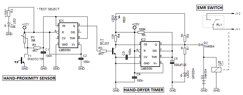
    Schematic circuit diagram of our 230V AC operated automatic hand-dryer is shown here. Since the electronic circuitry demands a stable 12V DC supply, make necessary arrangement to provide it from any self-made/ready-made linear or switch-moded power supply unit. The circuit is built around two LM555N chips (IC1&IC2);

    IC1 configured as medium-power inverting current driver, and IC2 as monostable multi-vibrator. When infrared light (IR) from the infrared light emitting diode (IR LED) falls on the phototransistor (T1), by reflection, output of IC1 goes to high level and this will switch IC2 through the BC237 transistor (T2). As a result, the electro-magnetic relay – EMR- (RL1) at the output of IC2 is energized to run the hand-dryer heater unit for a prefixed time period determined by the in-circuit values of RC timing components R5 and C5. The red LED (LED1) is the standby mode indicator, and the green LED (LED2) is the active mode indicator. The hand-proximity switching level can be adjusted with the 1M potentiometer (P1). The intensity of the infrared light source depends on the value of current-limiting resistor R2 (tested with 470R).
    Both the infrared light source and the phototransistor can be mounted side-by-side on a single panel. But, the infrared light source (IR LED) must be isolated from the phototransistor (T1) (using a small opaque sheet) to avoid false detection due to infrared leakage. The component values are not especially critical. However, the coil of relay RL1 must be have a low operating current, no more than a few dozen milliamperes.
    The entire circuit should be fitted in a well-insulated enclosure, since it is usually installed in a watery-area (rest room, bathroom, etc).

Monday, 5 January 2015

Battery Tester Project

Battery Tester Project Using LM3914 IC

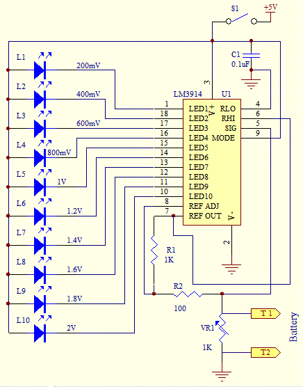
This objective of this project is to design and build a battery tester that is able to test various types of dry cell and rechargeable battery with a voltage of less than 2V. Configured as a bar graph battery level indicator, the LM3914 IC from National Semiconductor senses the voltage levels of the battery under test and drives the 10 LEDs to ON or OFF based on the voltage that is detected. The current driving the LEDs is regulated by using the external resistor R1 and hence limiting resistors are not required.
 he schematic shows the simple connections where the reference voltage at pin 8 of U1 can be adjusted by adjusting the variable resistor VR1. The voltage at pin 8 will set the maximum scale of the LED. In testing dry cell battery of 1.5V,set the voltage at pin 8 to 2.0V. Each of the LED will thus represent 200mV when lighted up.
Test the circuit by using a breadboard before soldering the parts onto the PCB. This is to ensure that all the components that are used are in working condition. This is one of the simplest and interesting project that you can embark on if you have not try any project using this integrated circuit and the use of light emitting diodes.
If testing of rechargeable battery such as NiCd or NiMH is required, set the reference voltage to a lower value such as 1.5V as the typical voltage of a rechargeable battery is approximately 1.2V.

When testing the battery, take note of the polarity of the probe to the terminals of the battery. T1 is to be placed on the positive terminal and T2 the negative terminal of the battery.


A digital or analog multimeter that is set to measure the voltage of the battery is necessary. The voltage that is measured is used as a standard against the voltage that is displayed on the LEDs.


ELECTRONICS STREET LIGHT SWITCH

ELECTRONICS STREET LIGHT SWITCH
Here is a simple, expensive and easy to use electronics street light switch using LDR and NE555. The working of this circuit is truly based on light sensing, i.e. automatic turn it on in night (no sunlight available) and turn It off at sunshine (sunlight available).

Circuit Description of Electronics street
light switch
As electronics street light switch is a switching circuit so, for more detail we can divide this circuit into two section i.e. power supply and switching circuit.

In this power supply section the work of step-down transformer is done by register R1 and further rectification to change into 9.1V dc is by diode D1 and zener diode ZD1. The output voltage across zener diode is further filtered by capacitor C1 and C2.

The another section  of street light is switching section built around light-dependent register LDR1 with the help of transistor T1 through T3 and timer IC NE555 (IC1), where LDR1 is used as sensor of this switching circuit.As in day time the resistance of LDR1 remain low but it is reverse in night time i.e. high resistance is offered by LDR1. For this property of LDR1 the timer IC used in this circuit is as inverter. So, high input at pin 3 is provided by low input at pin 2 and vice-versa. Lastly, this inverter is used to turn street bulb B1 on with the help of triac (triac is activated).
The transistor T1 and T2  is remain cut-off to make pin 4 and pin 8 of IC1 low due to light fall on LDR1 during day time. Due to this transistor T3 is also cut-off and trigger voltage is not received by IC1 through pin 2. As a result the output voltage at pin 3 is low which does not activate triac and the street bulb does not glow.